Since the conductance quantum e2/h contains only constants of nature, the conductance quantization might be expected to occur in metals as well as in semiconductors. A quantum point contact in a semiconductor is a mesoscopic object, on a scale intermediate between the macroscopic world of classical mechanics and the microscopic world of atoms and molecules. This separation of length scales exists because of the large Fermi wave length in a semiconductor. In a metal, on the contrary, the Fermi wave length is of the same order of magnitude as the atomic separation. A quantum point contact in a metal is therefore necessarily of atomic dimensions.If the initial contact between two pieces of metal is formed by a single atom, the conductance will be of the order of 2e2/h. This was first observed in 1987 by James K. Gimzewski and R. Möller (IBM, Zürich) [11], in experiments where the Ir tip of a scanning tunneling microscope was pressed onto a Ag surface. Upon making contact, the conductance jumped from an exponentially small value to a value of
. Later work, using mechanically more stable devices, showed that further jumps of order 2e2/h in the conductance occur as the contact area is increased.
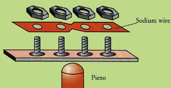
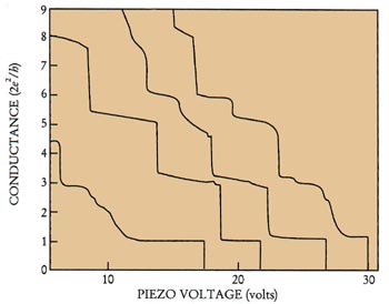
Figure 3. Quantized steps in the conductance of a Na point contact. A clean point contact is made at 4.2 K by breaking the wire at a notch cut across a thin wire, whereafter the two parts are brought into contact mechanically. The width of the point contact is adjusted by increasing the force of contact through a piezo element. Electrical measurements are made using four miniature brass bolts connected to the wire (see inset). The experiment is not fully reproducible, because of different atomic rearrangements in the contact region. (Adapted from ref. [12].)
Figure 3 shows experimental data for a Na point contact measured by Martijn Krans and collaborators from the Kamerlingh Onnes Laboratory in Leiden [12]. An adjustable contact of atomic dimensions, with a high mechanical stability, is made by bolting a notched wire of sodium onto a flexible substrate. As the substrate is bent, the wire breaks at the notch. The contact area can be controlled down to the atomic scale, simply by bending the substrate more or less. A statistical analysis of a large number of samples shows that, as the contact area is increased, steps in the conductance appear near 1, 3, 5, and 6 times 2e2/h. (Figure 3 shows the conductance steps for representative single measurements.) The absence of steps at 2 and 4 times 2e2/h is significant, and has a neat explanation: In a cylindrically symmetric potential the second and third transverse mode are degenerate, as are the fourth and fifth mode, while the first and sixth mode are non-degenerate.
The energy separation of transverse modes in a point contact of atomic dimensions is so large that the conductance steps are visible at room temperature. Nicolás García and his group at the Autonomous University of Madrid have made use of this property to develop a classroom experiment of quantized conductance. (See PHYSICS TODAY, February, page 9.)